【DRAM存储器二十五】DDR4介绍-DDR4 MR4-6详解,hPPR?存储单元失效了还能修复?

本文介绍了DDR4内存中的Hard Post Package Repair (hPPR) 和 Soft Post Package Repair (sPPR) 两种存储单元修复机制,以及它们的区别。此外,还讲解了DDR4的节能特性,如Temperature-Controlled Refresh模式、Command Address Latency和Maximun Power Savings Mode,以及Data Bus Inversion和Data Mask等功耗管理技术。

👉个人主页highman110

👉作者简介:一名硬件工程师持续学习,不断记录,保持思考,输出干货内容 

参考资料:《镁光DDR4数据手册》 、《JESD79-4B》

目录

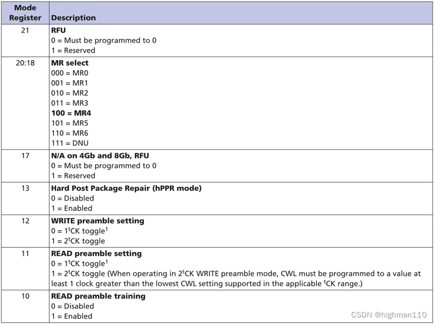
MR4
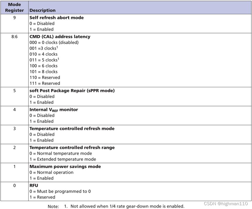
MR5

MR6


MR4

        1、Hard Post Package Repair (hPPR mode)

        翻译过来就是芯片封装好后的硬修复,就是颗粒已经贴装在用了,如果有存储单元失效,可以尝试用此功能修复。大家要注意,这里说的修复并不是说DRAM里有个存储单元已经坏了,比如说电容失效了,通过一些手段它能把这个电容修好,这显然是做不到的,所谓修复,其实只是把当前的失效点通过算法映射到DRAM冗余的存储点上,这样在外部看起来就是修复了一样。JEDEC规定这在4Gb颗粒是个可选功能,在8Gb及以上是必备功能,每个bank只能修复一行,也就是把失效的行映射到冗余的行上,且冗余行只有一个。由于hPPR是通过编程电熔丝来实现映射,所以


The DDR4 SDRAM is a high-speed dynamic random-access memory internally configured as sixteen-banks, 4 bank group with 4 banks for each bank group for x4/x8 and eight-banks, 2 bank group with 4 banks for each bankgroup for x16 DRAM. The DDR4 SDRAM uses a 8n prefetch architecture to achieve high-speed operation. The 8n prefetch architecture is combined with an interface designed to transfer two data words per clock cycle at the I/O pins. A single read or write operation for the DDR4 SDRAM consists of a single 8n-bit wide, four clock data transfer at the internal DRAM core and eight corresponding n-bit wide, one-half clock cycle data transfers at the I/O pins. Read and write operation to the DDR4 SDRAM are burst oriented, start at a selected location, and continue for a burst length of eight or a ‘chopped’ burst of four in a programmed sequence. Operation begins with the registration of an ACTIVATE Command, which is then followed by a Read or Write command. The address bits registered coincident with the ACTIVATE Command are used to select the bank and row to be activated (BG0-BG1 in x4/8 and BG0 in x16 select the bankgroup; BA0-BA1 select the bank; A0-A17 select the row; refer to “DDR4 SDRAM Addressing” on datasheet). The address bits registered coincident with the Read or Write command are used to select the starting column location for the burst operation, determine if the auto precharge command is to be issued (via A10), and select BC4 or BL8 mode ‘on the fly’ (via A12) if enabled in the mode register. Prior to normal operation, the DDR4 SDRAM must be powered up and initialized in a predefined manner. The following sections provide detailed information covering device reset and initialization, register definition, command descriptions, and device operation.
评论
成就一亿技术人!
拼手气红包6.0元
还能输入1000个字符
 
 条评论被折叠 查看
添加红包

请填写红包祝福语或标题

红包个数最小为10个

红包金额最低5元

当前余额3.43前往充值 >
需支付:10.00
成就一亿技术人!
领取后你会自动成为博主和红包主的粉丝 规则
hope_wisdom
发出的红包

打赏作者

highman110

你的鼓励将是我最大的创作动力!

¥1 ¥2 ¥4 ¥6 ¥10 ¥20
扫码支付:¥1
获取中
扫码支付

您的余额不足,请更换扫码支付或充值

打赏作者

实付
使用余额支付
点击重新获取
扫码支付
钱包余额 0

抵扣说明:

1.余额是钱包充值的虚拟货币,按照1:1的比例进行支付金额的抵扣。
2.余额无法直接购买下载,可以购买VIP、付费专栏及课程。

余额充值